Precision machining produces tiny, light-guiding nanocubes for advancing data tech (w/video)

Precision machining produces tiny, light-guiding nanocubes for advancing data tech (w/video)

[ad_1]

Jan 28, 2022

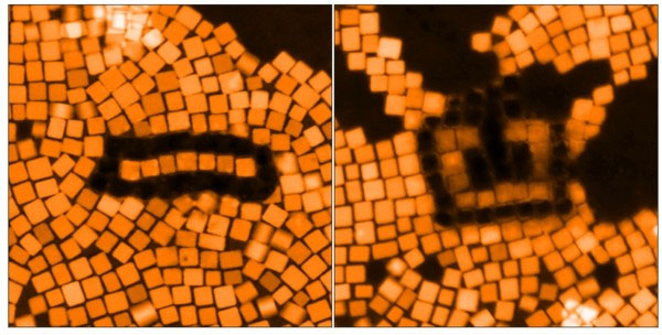
(Nanowerk Information) Drilling with the beam of an electron microscope, scientists on the Division of Power’s Oak Ridge Nationwide Laboratory exactly machined tiny electrically conductive cubes that may work together with mild and arranged them in patterned buildings that confine and relay mild’s electromagnetic sign. This demonstration is a step towards probably quicker pc chips and extra perceptive sensors. The seeming wizardry of those buildings comes from the power of their surfaces to assist collective waves of electrons, known as plasmons, with the identical frequency as mild waves however with a lot tighter confinement. The sunshine-guiding buildings are measured in nanometers.

“These nanoscale dice techniques permit excessive confinement of sunshine in particular places and tunable management of its vitality,” stated ORNL’s Kevin Roccapriore, first writer of a research printed within the journal Small (“Sculpting the plasmonic responses of nanoparticles by directed electron beam irradiation”). “It’s a technique to join indicators with very completely different size scales.” The feat could show essential for quantum and optical computing. Quantum computer systems encode data with quantum bits, or qubits, decided by a quantum state of a particle, resembling its spin. Qubits can retailer many values in contrast with the one worth saved by a classical bit. Gentle — electromagnetic radiation that propagates by massless elementary particles known as photons — replaces electrons because the messenger in optical computer systems. As a result of photons journey quicker than electrons and don’t generate warmth, optical computer systems might have efficiency and vitality effectivity superior to classical computer systems. Future applied sciences could use the very best of each worlds. “Gentle is the popular technique to talk with qubits, however you can’t join contacts to them straight,” stated senior writer Sergei Kalinin of ORNL. “The issue with seen mild is its wavelengths vary from about 380 nanometers for violet to round 700 nanometers for purple. That’s too huge as a result of we wish to make units just a few nanometers in dimension. This work goals to create a framework to maneuver expertise past Moore’s regulation and classical electronics. When you attempt to put ‘mild’ and ‘small’ collectively, that’s precisely the place plasmonics comes into play.” Precision machining produces tiny, light-guiding nanocubes for advancing data tech (w/video) ORNL scientists used an electron beam for precision machining of nanoscale supplies. Cubes have been milled to alter their form and may be faraway from an array. (Picture: Kevin Roccapriore/ORNL) And if there’s an awesome future in plasmonics, the ORNL-led achievement could assist overcome a sign dimension mismatch that threatens the combination of parts made of various supplies. These hybrid parts might want to “discuss” to one another in next-generation optoelectronic units. Plasmonics could bridge the hole. Plasmonic phenomena have been first noticed in metals, that are conductive due to their free electrons. The ORNL staff used cubes made from a clear semiconductor that behaves like a metallic — indium oxide doped with tin and fluorine. The truth that the dice is a semiconductor is the important thing to its vitality tunability. The vitality of a lightweight wave is said to its frequency. The upper the frequency, the shorter the wavelength. Wavelengths of seen mild seem to the human eye as colours. As a result of a semiconductor could be doped — that’s, a small impurity could be added — its wavelength could be shifted on the spectrum. The research’s cubes have been every 10 nanometers large, which is far smaller than the wavelength of seen mild. Synthesized on the College of Texas at Austin by Shin-Hum Cho and Delia Milliron, the cubes have been positioned in a detergent to forestall clumping and pipetted onto a substrate, the place they self-assembled right into a two-dimensional array. A shell of detergent surrounded every dice, spacing them aside evenly. After the detergent was eliminated, the arrays have been despatched to ORNL. “That the cubes don’t straight contact is vital for the collective habits,” stated Roccapriore, who organized the cubes into numerous buildings. “Every dice individually has its personal plasmon habits. Once we deliver them collectively in geometries like a nanowire, they discuss to 1 one other and produce new results that aren’t usually seen in related geometries that aren’t made up of particular person components.” nanocubes Every dice proven has its personal plasmonic habits. Carry them collectively in patterns — an antenna, left picture, or cut up ring resonator, proper picture — and so they “discuss,” producing distinctive results. (Picture: Kevin Roccapriore/ORNL) The research builds on prior work to sculpt three-dimensional buildings as small as a nanometer with an electron beam (“New electron microscopy technique sculpts 3-D buildings at atomic stage“). “The present paper proves that the plasmonic impact, in addition to the construction, could be sculpted,” Roccapriore stated. “On the finish of the day, we’re within the electron wave — the place is it and what’s its vitality? We’re controlling these two issues.” Kalinin added, “We wish to transition from utilizing what exists in nature by probability to fabricating supplies with the correct responses. We are able to take a system of cubes, shine mild on it and channel vitality into small volumes localized precisely the place we would like them to be.” The challenge was a pure for Roccapriore, who performed a whole lot of electron-beam lithography in graduate college and even constructed a machine in his storage to make and mill 3D-printed buildings. At ORNL, experimenting with the beam of an electron microscope, he adjusted its present to deliberately shift from imaging to modification mode. He discovered he might take away bits of cubes or complete cubes from an array to make patterned objects at will. He additionally found that, identical to addition of chemical components allows tuning of dice energies, so too does selective elimination of chemical components. Such atomic precision is feasible with scanning transmission electron microscopy, or STEM. The important thing to characterizing plasmonic habits inside single cubes and amongst collective dice assemblies was a way known as electron vitality loss spectroscopy. It makes use of a STEM instrument with an electron beam filtered to energies inside a slender vary. The beam loses vitality as its electrons cross by way of the pattern, work together with electrons within the materials and switch a bit vitality to the system by thrilling plasmons. “Electron vitality loss spectroscopy offers deep insights into unique physics and quantum phenomena associated to plasmonic habits,” stated co-author Andrew Lupini of ORNL, who helped map the energies of electrons within the cubes and arrays of cubes. Lupini is without doubt one of the builders of aberration-corrected STEM, which made pioneering advances attainable. “Electron vitality loss spectroscopy lets us analyze evolving plasmonic responses in actual time because the cubes are sculpted. We are able to determine relationships between preparations of cubes and their plasmonic properties.” The scientists plan to create a library of relationships between supplies, buildings and plasmonic properties. That new data will present the foundational understanding wanted to finally mass-produce buildings that may direct the stream of sunshine in plasmonic nanocircuits. In response to Roccapriore, “the concept is to know the relationships utilizing machine studying after which automate the method.”


[ad_2]

Previous Article

Did consuming meat actually make us human?

Next Article

BONUS: Drone Information - Drone Conferences in 2020, New Parrot Anafi Drone in Summer season 2020, Skydio 2 Updates, Safely Filming a Protest Utilizing a Drone

Write a Comment

Leave a Comment

Your email address will not be published. Required fields are marked *

Subscribe to our Newsletter

Subscribe to our email newsletter to get the latest posts delivered right to your email.
Pure inspiration, zero spam ✨