Scientists weave atomically skinny wires into ribbons

Scientists weave atomically skinny wires into ribbons

[ad_1]

Jan 29, 2022

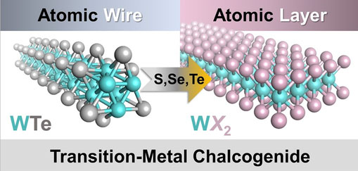
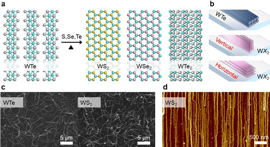
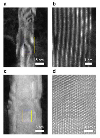
(Nanowerk Information) Researchers from Tokyo Metropolitan College have succeeded in utilizing nanowires of a transition-metal chalcogenide to make atomically skinny nanoribbons. Bundles of nanowires had been uncovered to a gasoline of chalcogen atoms and warmth which helped merge the threads into slender strips (ACS Utilized Nano Supplies, “Nanowire-to-Nanoribbon Conversion in Transition-Steel Chalcogenides: Implications for One-Dimensional Electronics and Optoelectronics”). Illustration of the transformation from nanowires to nanoribbons in transition-metal chalcogenides Illustration of the transformation from nanowires to nanoribbons in transition-metal chalcogenides. (Picture: Tokyo Metropolitan College) Nanoribbons are extremely wanted for stylish digital units; given the scalability of the strategy, the group hopes it should see widespread use within the industrial manufacturing of cutting-edge supplies. Supplies science within the electronics age is as demanding as it’s revolutionary. As circuitry get smaller, quicker, and extra power environment friendly, scientists are confronted with the more and more tough problem of controlling the atomic-level construction of the supplies which are utilized in them. One promising avenue of analysis is the usage of intricate threads of fabric just a few atoms extensive; one such construction consists of transition-metal chalcogenides, a mixture of transition metals and chalcogens, atoms which share a column with oxygen on the periodic desk. These atomically skinny “nanowires” possess properties distinctive to their one-dimensional construction and are extremely wanted for stylish digital units. However what they’ve in minuteness, they lack in tunability. That is the place “nanoribbons” are available in, that’s, slender, atomically skinny sheets. Fantastic management of their width, for instance, results in managed variation of their digital and magnetic properties. Schematic of nanowire to nanoribbon conversion process (a) Bundles of tungsten telluride nanowires are uncovered to a chalcogen vapor and heated, changing the bundles into slender, atomically skinny strips of transition-metal chalcogenide. (b) Bundles of nanowire could also be transformed into ribbons oriented each vertically and horizontally with respect to the substrate. (c) Randomly and (d) unidirectionally oriented nanoribbons could also be made utilizing totally different substrate materials. (Picture: Tokyo Metropolitan College) Quite a lot of work has been utilized to “construct” nanoribbons from the underside up. The issue, nevertheless, is that such strategies aren’t very scalable. That’s an issue for producing bulk portions for business units. Now, a group led by Dr. Hong En Lim and Affiliate Professor Yasumitsu Miyata from Tokyo Metropolitan College have give you a scalable manner of assembling nanowires into nanoribbons. The group had already pioneered methods to supply nanowires in bulk portions. By taking some tungsten telluride nanowires, they created bundles of wires deposited on a flat substrate. These had been uncovered to vapors of various chalcogens like sulfur, selenium and tellurium. With a mixture of warmth and vapor, the initially separate threads within the bundles had been efficiently woven collectively into slender, atomically skinny “nanoribbons” with a attribute zigzag construction. By tuning the thickness of the unique bundles, they might even select whether or not these ribbons had been oriented parallel to the substrate or perpendicular to it, due to a contest between how favorable it’s to have edges or faces parallel to the underside floor. Moreover, by tuning the substrate on which the bundles are positioned, they might management whether or not the ribbons had been randomly oriented or pointing in a single path. Vertically and horizontally oriented nanoribbon stacks (a,b) Vertically and (c,d) horizontally oriented nanoribbons, imaged utilizing transmission electron microscopy. (b) and (d) are close-up pictures of the areas marked in (a) and (c), respectively. (Picture: Tokyo Metropolitan College) Importantly, the strategy is scalable and could also be utilized to take the synthesis from lab-scale manufacture of some ribbons to bulk syntheses over massive substrate areas. The group had been in a position to affirm that the ribbons they created had the unique digital properties that are distinctive to their one-dimensional nature. Not solely is that this an enormous leap ahead for supplies science, however a tangible step in direction of seeing mass-produced nanoribbons in state-of-the-art electronics, optoelectronics, and catalysts.


[ad_2]

Previous Article

Starship Applied sciences raises $56M for supply robots

Next Article

Delta Drone Worldwide (ASX:DLT) to divest ParaZero for $6 million in money - sUAS Information

Write a Comment

Leave a Comment

Your email address will not be published. Required fields are marked *

Subscribe to our Newsletter

Subscribe to our email newsletter to get the latest posts delivered right to your email.
Pure inspiration, zero spam ✨