| Feb 04, 2022 |
|
(Nanowerk Information) Two of the primary drawbacks of utilizing tin (Sn)-based steel halide perovskites (MHPs) in thin-film transistors have been concurrently solved by an revolutionary hybrid 2D/3D construction proposed by scientists at Tokyo Institute of Know-how (Tokyo Tech). Their findings will assist unlock the potential of environmentally benign Sn-based MHPs in CMOS expertise, paving the best way for versatile and printable digital gadgets.
|
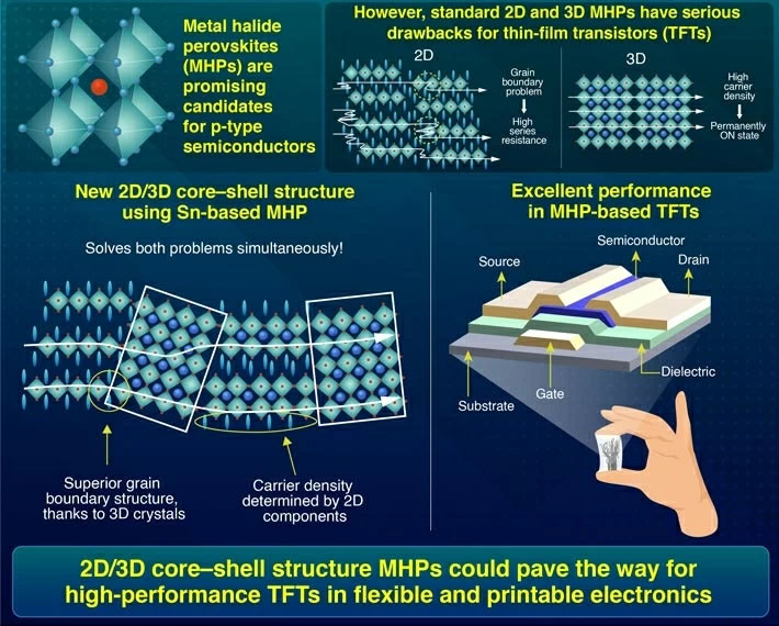 |
| Making Metallic–Halide Perovskites Helpful in Planar Gadgets By a New Hybrid Construction. (Picture: Tokyo Tech)
|
|
Metallic halide perovskites (MHPs) are a category of supplies with promising properties for semiconductor functions, reminiscent of thin-film transistors (TFTs). Particularly, tin (Sn)-based MHPs may very well be an environmentally benign various to lead-based ones, that are poisonous. Nevertheless, some essential points must be resolved earlier than Sn-based MHPs could be leveraged in planar semiconductor gadgets.
|
|
When organized right into a 2D construction (or quasi-2D construction with a couple of layers), defects within the crystal construction of Sn-based MHPs known as “grain boundaries” hamper the mobility of cost carriers all through the fabric. If utilized in a TFT, this phenomenon ends in a big collection resistance that finally degrades efficiency.
|
|
In distinction, a TFT made utilizing an Sn-based MHP organized right into a 3D construction faces a special but nonetheless crippling downside. The extraordinarily excessive service density of the 3D materials causes the transistor to be completely ON except very excessive voltages are utilized. Evidently, this renders such a tool ineffective for a lot of functions.
|
|
Luckily, a workforce of scientists from Tokyo Tech, Japan, have discovered an answer to those limitations. In a current examine revealed in Superior Science (“Excessive-Efficiency P-Channel Tin Halide Perovskite Skinny Movie Transistor Using a 2D–3D Core–Shell Construction”) and led by Assistant Professor Junghwan Kim and Honorary Professor Hideo Hosono, the researchers proposed a novel idea primarily based on a hybrid construction for Sn-based MHPs, known as the “2D/3D core–shell construction.”
|
|
On this construction, 3D MHP cores are totally remoted from each other and linked solely by quick 2D MHP strips (or “shells”). This alternating association solves each of the abovementioned drawbacks concurrently. However how?
|
|
The trick to reducing the collection resistance of 2D MHPs is to eradicate the service mobility issues at grain boundaries, that are attributable to misalignments between the conductive octahedra of the perovskite. Because of the best way wherein the 3D cores hook up with the 2D segments, these misalignments disappear and the collection resistance is vastly lowered.
|
|
As for the excessive service density of 3D MHPs, this downside is solely not current when utilizing the 2D/3D core–shell construction. Because the 3D cores are remoted, their service density is not related; as a substitute, the 2D segments act as a bottleneck and restrict the efficient service density of the general materials.
|
|
To exhibit the effectiveness of this novel construction, the workforce fabricated a complementary steel–oxide–semiconductor (CMOS) inverter by combining 2D/3D TFTs with a regular indium gallium zinc oxide TFT.
|
|
“Our gadget exhibited a excessive voltage acquire of 200 V/V at a drain voltage of 20 V. This efficiency is the perfect reported to this point for a CMOS inverter made utilizing Sn-MHP TFTs,” highlights Prof. Kim.
|
|
The revolutionary 2D/3D construction introduced on this examine will assist scientists worldwide make the most of the enticing digital properties of perovskites. Furthermore, their strategy will not be restricted to a slender class of supplies or gadget varieties.
|
|
“The proposed technique may very well be utilized to numerous solution-derived semiconductor programs, opening doorways to versatile and printable electronics,” says Prof. Kim.
|